Mikrostrukturierte Titan-Oberfläche unter dem Mikroskop.

Imagine a world in which tiny structures improve the performance of entire systems. Whether in medical implants, optical lenses or highly sensitive microsensors – this is exactly where microstructuring comes in. It makes it possible to specifically modify materials in the micrometer range and thus give them new and functional properties.

What initially sounds complex is actually a crucial component for many modern applications. Companies in the fields of medical technology, electronics and micromechanics are increasingly relying on microstructured surfaces to combine precision, efficiency and miniaturization.

In this article, you will find out what microstructuring really means, which processes are currently being used and how these technologies work in practice. We shed light on materials, fields of application and typical challenges. We combine comprehensible specialist knowledge with specific application examples and provide you with decision-making aids to help you exploit the full potential of this technology.

By the end of this article, you will not only understand why microstructuring is considered a key technology in many industries, but also recognize how it can be used to achieve measurable benefits.

Table of contents

Why microstructuring is more important today than ever

Comparison of conventional vs. microstructured surface of a surgical instrument

Products are continuously becoming smaller, lighter and at the same time more powerful. This is leading to new requirements, particularly in medical technology. This results in instruments with particularly fine geometry and specifically structured surfaces that damage less tissue and can be cleaned more quickly.

Precision in demanding industries

  • Medical technology: Instruments benefit from improved surfaces for greater safety and effectiveness.
  • Optics: Structured microprofiles specifically control light propagation and enable new functions.
  • Semiconductor technology: The finest structures allow the integration of complex functions in the smallest of spaces.

In all these areas, microstructuring delivers reproducible and precisely controllable results – a real competitive advantage in markets with high quality requirements.

New materials require new methods

Biocompatible plastics, high-strength alloys or ceramic materials place special demands on machining. Traditional processes reach their limits here. Modern technologies are needed that can work without mechanical pressure and at the same time produce structures with micrometer precision.

Microstructured surfaces open up precisely these possibilities. They increase the service life of technical components, improve the adhesion of coatings and enable controlled fluidics in channels and micro-cavities.

Technologies with a future

Processes such as additive manufacturing significantly increase design freedom. In combination with microstructuring, functional surfaces are created directly during production. This saves resources and allows new design approaches.

Intelligent surfaces that actively react to environmental conditions are particularly exciting. Temperature, light or humidity change the function in a targeted manner – a development that is becoming increasingly important. And it starts exactly where the microstructure makes the difference.

Good to know - advantages of microstructuring

Processes and applications in medical technology

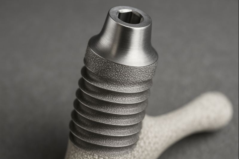
In medical technology, every detail influences the function and safety of a product. A targeted microstructure of the surface can make all the difference. Implants, for example, benefit from improved cell adhesion and precisely defined coefficients of friction. Structured titanium or ceramic surfaces have a targeted effect on biological processes, promote healing, reduce the risk of inflammation and increase stability over longer periods of time.

Structures for surgical instruments

Surgical tools are subject to different requirements. In addition to mechanical strength and biocompatibility, cleanability is also crucial. Microstructuring creates functional zones directly on the surface. This makes it possible to integrate non-slip areas for a better grip or slippery sections for low-friction movements. This optimization increases safety and improves handling in clinical use.

Close-up of a lab-on-a-chip system with microfluidic structures

Microfluidics and drug release

Another important field of application is the development of microfluidic components. State-of-the-art laser technology is used to create precise channels and openings in biocompatible materials. Such structures are used in diagnostic devices, dosing systems for medicines or in so-called lab-on-a-chip solutions. Microneedles and porous surfaces for controlled drug delivery are also based on these processes.

Fine machining of sensitive materials

The electrical discharge machining process is ideal for particularly delicate instruments. Wire erosion enables the processing of conductive high-performance materials without mechanical impact. This allows extremely thin-walled components to be produced with precise geometry and outstanding surface quality. This method is ideal for instruments used in ophthalmology or for minimally invasive procedures.

Molding tools with integrated structure

Die-sinking EDM is often used in the production of tool molds, for example for plastic injection molding. This allows microstructured areas to be incorporated directly into the mold. The result is plastic components with specific functionality. A typical example is a catheter sheath with a water-attracting surface or a dosing opening with a precisely controllable flow rate. The structure is created in the mold and is thus integrated directly into the production process.

Practical example: Spinneret for pharmaceutical applications

A manufacturer from the pharmaceutical sector developed a spinneret to produce ultra-fine fibers. These were to serve as a carrier medium for active medical ingredients. The component was manufactured using wire erosion. The decisive factor was the precise shaping of several parallel outlet channels with an exactly defined geometry. The finished nozzle ensured uniform fiber formation with minimal tolerance. The result was a robust, highly functional component for series production.

Fields of application: Where microstructuring creates real added value

Optical industry: precise control of light

Microstructuring is a key tool in the optical industry for controlling light. Reflection, scattering and light transmission can be influenced through targeted structuring without having to change the external shape of a component. Among other things, this enables

– Lenses with integrated anti-reflection zones
– Light guides for miniaturized systems
– Surfaces that filter specific wavelengths

Such structured surfaces are indispensable in the production of high-precision optical parts such as diffraction gratings or Fresnel lenses.

Microstructured lens with anti-reflective coating
Close-up of a lens with fine anti-reflective structures

Semiconductor technology and sensor development

In the field of semiconductors and sensor technology, microscopically small structures determine performance and function. Microstructured surfaces not only enable a more compact design, but also open up new possibilities such as:

  • – Targeted control of heat flows
  • – Integration of conductive or insulating functional layers
  • – Higher sensitivity and selectivity for sensors

This technology ensures more accurate measurements and more robust systems, particularly in medical and environmental technology.

Micromechanics: Precision in the smallest space

In micromechanics, functionality and durability are required with a minimum component size. Microstructuring contributes to this,

  • – Reduce friction
  • – Efficient integration of lubricant depots
  • – generate specific strength curves in components

Components such as gear wheels, levers or springs benefit from this form of structural control. They retain their dimensional stability and function even under permanent load.

Piezo technology: Reaction to pressure and movement

In piezo technology, structured materials enable targeted conversion of mechanical energy into electrical energy. Microstructuring supports the development of:

  • – Actuators with defined motion response
  • – Ultrasonic transducers for precise sound transmission
  • – Sensitive tactile surfaces

Functional integration as the key

All of these fields of application share a common goal: to integrate functions directly into the surface. This reduces the need for additional components. The results are more compact, more efficient and more powerful systems that are optimally adapted to their area of application.

Overview of microstructuring methods

Various workpieces - manufactured with laser, erosion, lithography

Various technologies are available for the production of microstructured components. Each method offers particular strengths and is subject to certain limitations. The choice depends on the respective material, the desired structural shape and the economic requirements.

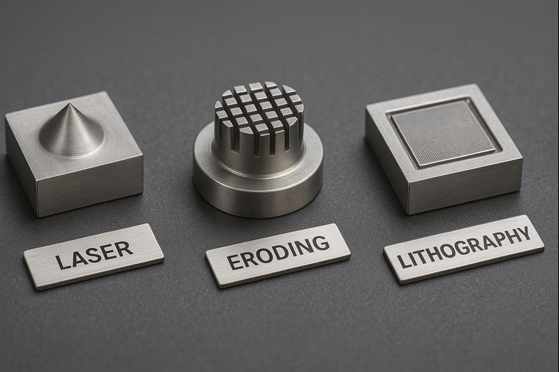
Laser-based processes

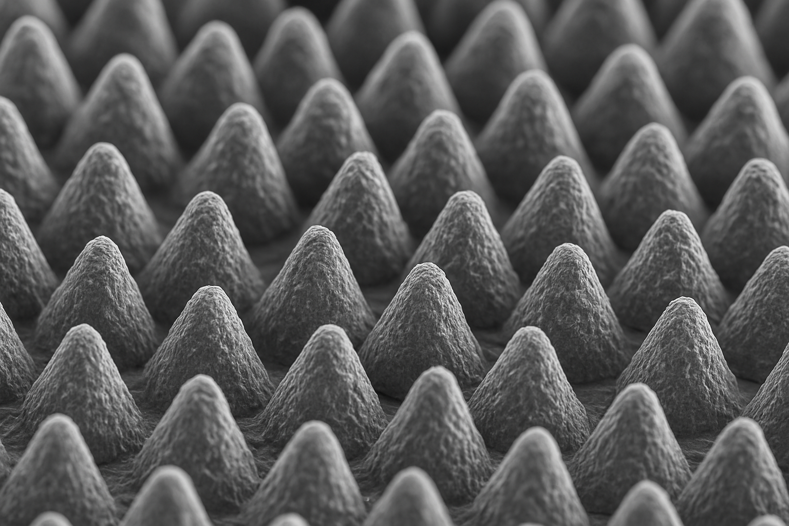
Laser structuring is one of the non-contact technologies with very high precision. A focused beam of light removes material in a targeted manner or changes it by heating it at specific points. Depending on the pulse duration and the wavelength used, structures with a very fine resolution can be created – from a few micrometers to complex three-dimensional geometries. This method is particularly suitable for sensitive materials such as ceramics or certain plastics, as the material stress remains low.

Chemical processes for precise patterns

Etching and lithography are based on the use of masks that are previously applied to the material. After exposure, the material is treated with specific chemical substances such as acids or alkalis. This creates precisely defined channels or cavities. These processes are ideal for repeatable structures on larger surfaces, for example in the manufacture of sensors or microprocessors. Their particular strength lies in the ability to depict highly complex patterns with extreme accuracy.

Machining technologies for flexible applications

Micro-milling and micro-cutting are suitable for materials that are easy to machine mechanically. With modern CNC systems, fine engravings, channels or fits can be realized directly in metals or plastics. These methods offer a high degree of flexibility, but the achievable depth and level of detail depend on the material and tool.

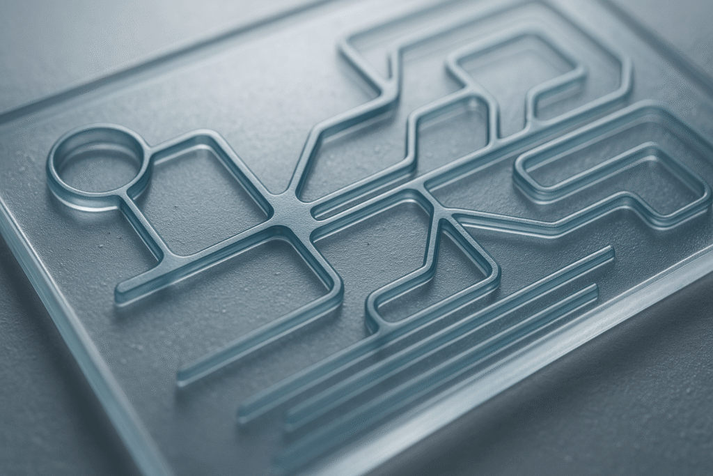
Electrochemical and spark erosion processes

Electrochemical processing methods and electrical discharge machining are particularly relevant for materials with electrical conductivity. During erosion, material is removed by targeted electrical discharge. As no mechanical forces act on the workpiece, the geometry remains stable even with very hard materials such as titanium or carbide. These processes allow extremely fine contours, tight tolerances and clean inner surfaces.

The right combination makes all the difference

No method is universally applicable. The key often lies in combining different methods. Not only can technical goals be better achieved, but economic advantages can also be exploited. Careful planning that takes all aspects into account – from the geometry to the material and series production capability – is crucial.

Materials and their suitability for microstructuring

The choice of the right material is a decisive factor for the success of microstructured components. Not every material reacts in the same way to temperature changes or mechanical processing. The decisive factor is the combination of formability, stability and functional benefits.

Ceramics – stable under extreme conditions

Ceramic materials impress with their high chemical and thermal resistance. They are particularly suitable for applications involving extreme temperatures or aggressive media. However, their brittle nature requires special processing methods. Processes without direct contact such as laser processing or spark erosion technologies are particularly advantageous here. The structures remain permanently stable and show only minimal wear.

Silicon – the all-rounder in microelectronics

Silicon forms the basis of numerous microelectronic systems. It can be excellently structured using lithographic and chemical processes and offers ideal conditions for precise, planar structures. Thanks to its low thermal expansion and electrical conductivity, silicon is the first choice for many applications in microelectronics and sensor technology.

Polymers – flexible in form and function

Polymers score points for their wide variety of shapes and ease of processing. They can be structured using thermal shaping, milling, etching or laser processes. Biocompatible plastics such as PEEK or PMMA are frequently used in medical technology. They enable targeted drug delivery and improve cell interaction. One challenge lies in the limited heat resistance and dimensional stability under changing conditions.

Metals – robust and versatile

Metallic materials such as stainless steel, titanium or aluminum impress with their high mechanical strength and electrical conductivity. They can be machined and electrochemically processed. Titanium in particular is valued for its biocompatibility and corrosion resistance for implants and medical tools. Stainless steel is particularly suitable for series production. Aluminum is well suited for initial prototypes or complex functional samples.

Important material properties at a glance

  • Thermal sensitivity: influences the choice of process
  • Dimensional stability: determines the dimensional stability of the structure
  • Hardness: influences the choice of tool and processing time
  • Wear behavior and chemical resistance: are decisive for long-term use
  • Conductivity: enables additional processing methods such as electrochemical ablation

Biocompatibility in medical technology

Compatibility with the human body is particularly important in medical technology. The selected microstructure must not only be functional, but also harmonize well with tissue, fluids and cleaning procedures. Surfaces with a specifically enlarged contact area, defined roughness or special coatings contribute to better biological integration and increase the probability of success in use.

From idea to implementation: the process of microstructuring

Steps of microstructuring - process graphic

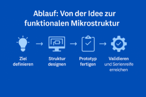
Step 1: Target definition and structure design

It all starts with a clearly formulated goal. This may involve optimized flow properties, precise sensor functions or a bioactive surface for implants. The first development step is the structural design. Specialized design software and digital simulations are used to create models that realistically depict the behaviour of the planned structure. Aspects such as light distribution, flow behavior or mechanical stress are already analyzed and improved at this stage. This significantly reduces time, costs and potential sources of error in the subsequent production process.

Step 2: Building and validating the prototype

The next step is prototype construction. Different technologies are used depending on the objective and the material used. Examples include laser processes, milling technology or chemical structuring. The samples created are thoroughly tested: Dimensions, surface quality and functionality must correspond exactly to the specifications. Consistent quality management ensures complete traceability. Even the smallest deviations in the micrometer range can impair the function and are therefore consistently documented.

Step 3: Transition to series production

Once the prototype has been approved, the scaling phase begins. The switch from one-off production to series production places high demands on reproducibility and process control. Only stable and automatable production methods enable reliable series production. Systems with high processing speed, precise monitoring and reproducible positioning are important here. The material supply, any reworking and testing processes must also be integrated into a seamless overall concept.

Step 4: Cooperation as a success factor

A successful project is based on close coordination between development, production and quality assurance. Early coordination prevents unnecessary correction loops and ensures cost-effective results. Cooperation with experienced production partners is particularly advantageous. They not only contribute technical knowledge, but also sound experience in dealing with complex materials and demanding applications.

Conclusion: Structured process with a clear goal

The development of microstructured solutions is challenging, but can be easily mastered through clearly defined steps. Those who plan consistently, test in good time and rely on stable technologies lay the foundation for functional, scalable and marketable products with long-term benefits.

Challenges and typical concerns in microstructuring

Limits and stumbling blocks in detail

Microstructuring offers enormous potential, but also specific challenges. A frequent stumbling block is the choice of material. Not every base material can be processed reliably and dimensionally stable on the desired scale. Soft plastics show a high tendency to deform when exposed to heat. In contrast, brittle ceramics place high demands on the process, as they need to be treated particularly gently. If the wrong method is chosen here, there is a risk of unstable results, production rejects or unnecessary cost increases.

Thermal effects as a risk factor

Another critical point is thermal influences during structuring. Working with laser beams or heated tools in particular can lead to undesirable changes in the material. These include hardening, internal stresses or minimal deformations. These can have a negative impact on dimensional accuracy or the functionality of sensitive components. Choosing the right processing parameters such as pulse duration, energy intensity and beam quality is therefore essential.

Cost-effectiveness and scalability

Cost is a key issue for many companies. Microstructured surfaces require precise processes that are associated with corresponding costs. This technology becomes economically interesting above all when large quantities are produced or the structure offers a clear functional advantage. A careful cost-benefit assessment should therefore be carried out at the start of any planning. Small series or pilot projects can help to identify risks at an early stage and recognize potential for optimization.

Case studies and industry solutions from practice

Real projects show how broadly and effectively microstructuring can be used in practice. Each example illustrates the direct benefits of the technology for function, safety or production quality – precisely tailored to the respective application.

Implant with bioactive surface

A manufacturer of orthopaedic implants was pursuing the goal of significantly reducing the healing time of its titanium components. The solution lay in the targeted structuring of the contact zones. Modern laser technology was used to apply a microporous geometry that improves cell adhesion and supports tissue growth. The result: significantly increased biological compatibility and more stable anchoring in the bone. Clinical tests have shown a demonstrably shorter healing time with the same stability.

Bone implant with structured contact surface
Example: Titanium implant with a specifically microstructured surface for cell adhesion

Lens with optimized light guidance for medical diagnostics

A company from the imaging technology sector developed a system for analyzing skin surfaces. The aim was to reduce interfering reflections while at the same time optimizing light guidance. The solution was a microstructured anti-reflection coating directly on the lens surface. This was created using ultra-short laser pulses. The result was a uniform light distribution with improved contrast. The structure was so precisely tuned that it did not impair the optical system – while at the same time increasing the precision of the imaging.

Stainless steel sensor housing for cleanroom use

A manufacturer of highly sensitive microsensors was looking for a housing with a high level of impermeability and cleanroom suitability. The choice fell on stainless steel, processed using an electrical discharge machining process. This resulted in precise housings with sharp inner edges and smooth, particle-free surfaces. These properties were decisive for the subsequent integration into a modular sensor system. The manufactured components met both mechanical and hygienic requirements at the highest level.

These examples make it clear that microstructuring is far more than just a theoretical possibility. It is a practical tool for solving complex technical requirements. The combination of material expertise, precise technology selection and application-oriented implementation is crucial. Only this interplay creates measurable added value – repeatable, reliable and industrially usable.

Ready to turn your idea into reality?

Together we realize solutions that work - precise, scalable and economical.

Why expertise counts and what distinguishes good providers

If you want to fully exploit the potential of microstructuring, you need more than just modern production technology. An understanding of processes, materials and specific areas of application is crucial. An experienced service provider recognizes at an early stage which technology suits the task and which errors must be avoided at all costs.

Specialist knowledge is more important than the machine inventory

Even the most modern systems do not guarantee optimum results. The decisive factor is know-how in the practical use of the processes. Questions such as: How does a certain material react to short laser pulses? Which structures can be reliably produced under clean production conditions? Such considerations require extensive practical experience – far beyond the mere control of the device. In demanding projects, application-oriented knowledge is often more valuable than pure machine technology.

Certified processes as a sign of quality

Professional suppliers work according to validated processes and in compliance with recognized standards. Certificates such as ISO 13485 in the field of medical technology or ISO 9001 for general manufacturing are proof of structured quality management. In addition, comprehensible process documentation, test certificates and transparent traceability are important characteristics of reliable partners. Especially in regulated industries, these standards create security – and a solid basis for long-term business relationships.

Avoid typical mistakes when selecting service providers

  • Too strong a focus on price: A low-cost offer is of little use if components are not manufactured to size or surfaces are not consistent.
  • Lack of feasibility analyses: Suppliers who start production directly without prior testing increase the risk of rejects or unnecessary corrections.
  • Unclear communication: Good partners ask precise questions, offer sensible alternatives and actively support the customer in finding a solution.

A decisive advantage often lies in the detail: Those who communicate clearly, respond flexibly to requirements and are aware of technical alternatives deliver better results in the long term. In such cases, not only does trust develop – joint innovative strength also grows.

In the end, it is not just the technology that is decisive. It is the people and processes behind it that turn a vision into a functioning product. Those who rely on experience, a systematic approach and open collaboration gain twice over: in terms of security and future viability.

From theory to practice: Where can you find precise microstructuring with vision?

When it comes to microstructured solutions for the most demanding requirements, it quickly becomes clear who offers real expertise. The decisive factor is not only the technical implementation, but also the interplay of sound advice, in-depth understanding of the industry and comprehensive manufacturing expertise. RETERO GmbH has positioned itself as a reliable partner for companies in the medical technology, optics, semiconductor technology and micromechanics sectors.

Thinking ahead starts with the design

RETERO supports projects not only during production, but also in the early stages of development. Materials, tolerance limits and functional details of the microstructure are thought through together with the customer. The goal is a solution that not only functions technically, but is also stable, economical and application-optimized in the long term. This forward-looking approach reduces development cycles and lowers production costs in the long term.

Broad range of technologies for customized solutions

  • Internal geometries with maximum precision: realized by wire EDM, ideal for delicate, conductive materials.
  • – Cavities with clear edges: Created by die-sinking erosion, even with difficult materials.
  • – Functional surfaces: Laser-structured areas, precisely matched to the application and active principle.

At RETERO, every project is considered individually. Simulation, analysis and verification are standard. The strength lies not in the use of a single method, but in the combination of all available technologies – intelligently networked and reliably controlled.

Experience with standards and regulatory requirements

Compliance with standards is crucial, especially in medical technology. RETERO knows the industry-specific requirements in detail. Biocompatibility, traceable documentation and validatable processes are standard here. ISO 13485 and ISO 9001 certifications prove the consistent implementation of quality assurance in all process steps.

More than just a paver: your development partner

If you want to use microstructuring strategically, you need more than just manufacturing. RETERO offers entrepreneurial thinking coupled with technological depth. The company sees itself as a co-creator of innovative solutions – for products that stand out from the competition. This is where precision and practice meet experience and future orientation.

Conclusion: Microstructuring – small structures, big effect

The trend towards ever more compact systems is no longer a marginal issue. It is shaping numerous industries and is becoming increasingly important. Requirements are increasing, particularly in medical technology, optics and micromechanics: Products need to be smaller, more powerful and at the same time more flexible to use. This is precisely where microstructuring comes in. It creates functional surfaces in the smallest of spaces and brings physical properties into harmony with technical and economic objectives.

From surface to function

What was once considered a technological gimmick is now an integral part of advanced product development. Microstructured surfaces not only perform protective or decorative functions. They are active:

  • – influence flow behavior in microfluidic systems
  • – increase sensor sensitivity through targeted light control
  • – promote cell growth in implants
  • – reduce friction or wear thanks to optimized geometries

All of this takes place in an extremely limited space – an advantage that has technological and economic relevance.

A clear advantage for innovative companies

Microstructuring opens up clear opportunities for companies. Those who invest in specialist knowledge, advanced manufacturing technologies and stable processes today are not only strengthening their own innovative power. They also position themselves competitively in the long term. This is not just about access to technology, but above all about the ability to translate specific requirements into functioning product solutions.

More than just a tool: a key to the future

Microstructuring is not a short-term fashion. It is constantly evolving – with every new class of material, every application and every product idea. It enables sustainable, safe and intelligent products that set new standards. Those who combine quality, understanding of materials and process control are actively shaping the future – not only technically, but also economically.

Frequently asked questions (FAQs) about microstructuring

What is microstructuring?

Microstructuring refers to the targeted modification of surfaces or materials in the micrometer range in order to improve certain physical, mechanical or biological properties.
Not necessarily. Whether a microstructure makes sense depends heavily on the planned function, the material used and the geometric shape. A thorough analysis in advance is essential.
It improves cell adhesion, shortens the healing time of implants, enables microfluidic systems and increases the cleanability of surgical tools.
The most important processes include laser structuring, etching, lithography, micro-milling, electrochemical machining and spark erosion methods such as wire erosion or die sinking.
Suitable materials include ceramics, metals such as titanium and stainless steel, polymers such as PEEK and semiconductor materials such as silicon – depending on the desired area of application and structural detail.
Depending on the method, structures down to less than one micrometer are possible. Lithographic and optical processes in particular offer the highest resolution.
Yes, especially for medium to high quantities or when functional advantages such as friction reduction or optimized fluidics significantly increase the added value.
In many cases, yes. The prerequisites are automatable process parameters and qualifiable results, especially for series production.
Medical technology, optics, semiconductor technology, micromechanics, piezo technology and environmental technology are among the main users of microstructured components.
Incorrect material selection, thermal damage, imprecise processes or a lack of process stability can lead to rejects or loss of function.
The costs vary greatly depending on the process, structure size, material and quantity. An individual offer is generally sensible and recommended.
Look for experience, industry knowledge, certified processes (e.g. ISO 13485) and the ability to provide process-oriented advice and implementation.